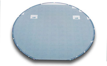
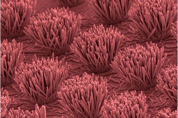
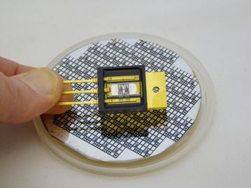
X-ray detectors
There is a need for x-ray detectors offering an extreme resolution and contrast at low x-ray doses.
A new x-ray detector concept has been developed at KTH and commercialized by Scint-X, specially suited for, e.g., dental applications and for integration in production lines. The x-ray detectors are based on a silicon structure where pores are etched to confine the light produced by a scintillator on a detector array.
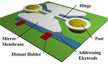
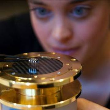
Micromirrors
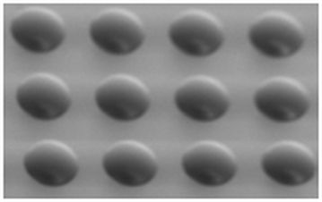
Micromirrors made on substrates of monocrystalline silicon offer minimal hysteresis and memory effects, and extreme flatness, optical quality and uniformity. The challenge is to monolitically integrate micromirrors with conventional silicon CMOS.
At KTH large arrays of IC integrated mono-crystalline silicon micro-mirror arrays for maskless lithography systems and adaptive optics systems are developed.
For more information:
KTH

Nanowire biosensor
Highly sensitive biosensors are used for medical diagnosis, bioprocess industry and environmental monitoring.
KTH and RISE have developed an electrical biosensor, based on the fact that biomolecules binds selectively to specific antibodies, using nanowire transistors and microfluidics technology with extreme sensitivity suitable for portable biosensing instruments.
Highly efficient heat exchangers
Efficient transfer of heat over a metal plate is of tremendous importance for heat exchangers in industrial cooling and heating applications, home refrigeration, etc.
A surface modification method for enhanced heat transfer has been developed by KTH and commercialized in the spin-off company µΔT (MicroDeltaT). The structure is micropourous with nano-sized voids in a copper plate.
Nanoparticles for drug delivery
Nanoparticles could be used as a vehicle to deliver medicines to precisely defined cells and tissue. This will reduce the amount of active substance needed and the risk of side effects.
KTH has developed multifunctional nanoparticles, which are targetable, biodegradable, traceable in vivo and equipped with controlled drug release for this purpose.
For more information:
KTH
Photonic crystals
The ability to control light in the same manner as electricity is controlled in integrated electronics, enables highly efficient integrated photonic devices, comprising novel waveguiding solutions and light detection systems .
Photonic crystals is a periodic structure with nanometer precision which interacts with the light waves. By high precision fabrication methods KTH has developed advanced photonic crystals both for integrated optic devices and to obtain negative refraction.
Silicon quantum dots
Quantum dots are one dimensional structures in the nanometer scale, exhibiting quantum mechanical properties.
Quantum dots based on silicon with a dielectric cap layer of silicon dioxide are fabricated and characterized in order to reveal their detailed photophysical properties, e.g., spectral fine-structure, excitonic lifetime and emission saturation.
For more information:
KTH
Nanophotonics for energy applications
The need for efficient light generation and light harvesting devices will continue to be a major driving force both for research and for business.
KTH focuses on the investigations of new concepts in light-matter interaction together with disruptive technologies for efficient photovoltaic and light emitters. This includes research on nano-wire/nano-pillar solar cells in III-Vs and Si, low-cost nanostructuring methods and plasmonic solar cells.
For more information:
KTH
Electronics for extreme conditions
The ability to place electronics at places with extremely high temperature or fatal radiation will open for entirely new applications for both industry and research.
KTH develops electronic circuits in silicon carbide, a material which may withstand temperatures up to 600ºC and environments with high radiation levels. Silicon carbide electronics may be used in oil and gas drilling, engines, nuclear power plants and even in outer space.
For more information:
RISE

Nanotransistors for high speed electronics
The ever decreasing dimensions of transistors aims at faster, smaller and more energy efficient electronics.
KTH conducts research on silicon based MOSFET transistors for future emerging nanoelectronics, as physical dimensions approach a few nanometer feature size. A range of technologies have been developed, e.g., Sidewall Transfer Lithography technology, which enables extremely low edge roughening also at narrow linewidths, and epitaxial growth of Si/SiGe heterostructures with controlled strain.

Silicon carbide high power electronics
Compact, robust and low loss high power electronics is of fundamental importance in a variety of applications. Power efficiency and compact size is important for, e.g., inverters for photovoltaics and electrical vehicles.
KTH and RISE has a long history in silicon carbide high power electronics research and today Fairchild Semiconductors refines and commercializes the device technology. RISE has started the Acreo SiC Power Center, a platform for cooperation between industry, research institutes and academia offering full scale competence and knowledge in power electronics.
Recycling thermal energy
Thermal energy, which today is wasted in millions of cars, airplanes and factories around the world, can be harvested and recycled to lower fuel consumption and to improve the efficiency of solar cells when the sun light is missing.
Nocilis Materials has developed energy harvesting devices based on a low cost, environmental friendly silicon material technology which also enables mass volume production. In addition Nocilis Materials provides epitaxial services.
Telecommunication lasers
Telecommunication for fiber-to-the home applications demand extremely reliable lasers operating at high frequency and high power, allowing cost efficient manufacturing.
KTH develops a new generation of single mode vertical cavity surface emitting lasers with state-of-the-art performance including high single mode power, ultra-high direct modulation bandwidth and excellent temperature stability.
For more information:
KTH
Photonic integrated circuits
The ever increasing internet traffic puts demands on the broadband capacity.
KTH is active in developing integrated photonic circuits, where a range of optical devices, e.g. lasers, detectors, modulators and wavelength converters are interconnected on a single chip to improve the efficiency of internet. A unique process available at KTH is the Hydride vapor phase epitaxy, which enables highly planar regrowth of crystalline material on non-planar substrates. This is a key-process for integration of photonic devices into larger circuits.
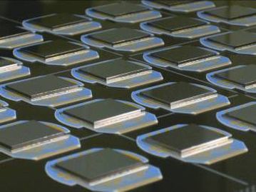
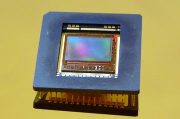
Imaging detectors
New generation imaging devices for non-visible wavelengths are highly demanded for many civil and military applications.
RISE develops new detectors and detector arrays for imaging applications at non-visible wavelengths (X-ray, UV and IR) in frame of the Institute Center of Excellence IMAGIC. The detectors are designed and fabricated utilizing advanced semiconductor materials and fabrication technologies. They can be integrated with CMOS read-out circuits.
For more information:
RISE
Infrared imaging detectors
Infrared (IR) detectors are used in a variety of applications; for surveillance in darkness or dusty environments, for process control and detection of heat leakage from buildings.
RISE has developed and refined the Quantum Well Infrared Photodetector technology to perfection and the detectors are now commercialized by IRnova. In addition to the conventional heat detection applications at different wavelengths, also a highly specialized imaging detector for SF6 gas leakage is available.
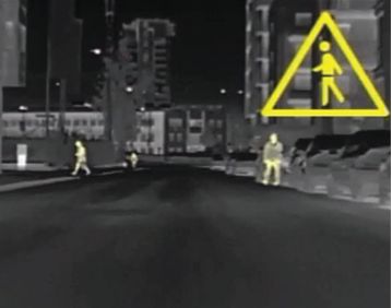
Microbolometer for automotive safety
Improved night vision helps the car driver to recognize pedestrians and animals on the road, but cheap solutions are required to make the technology available for most drivers.
KTH and RISE have developed imaging sensor technology with excellent performance, based on advanced microsystem- and nanotechnology. These sensors are suitable for automotive night vision an also for detection of warm objects in general surveillance. The cost is significantly reduced as compared to current technology.
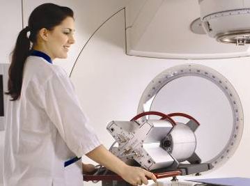
Component in cancer treatment system
Radiotherapy systems in the pre-treatment phase lack directional-independent detectors for the treatment of brain tumors.
RISE and Scandidos have developed a detector that can be used in future cancer treatment equipment.
UV sensing components
Low cost and robust UV detection devices are highly desirable in applications of flame sensing, fluorescence-based biochemical sensing, air, water and food inspection, and biomedical instrumentation needs.
RISE has worked on various UV detectors based on wide-bandgap semiconductor materials (silicon carbide, gallium nitride, and zinc oxide). These have the potential to provide very sensitive, compact and low cost solutions for UV detection and imaging.
For more information:
RISE
Nanorods for detection of ultraviolet (UV) light
Imaging UV detectors may be used in a wide range of applications, such as flame detection, surface inspection of roughness and scratches, and for identification of bacteria and biological organisms.
RISE investigates a fabrication method of one dimensional zink oxide nanorods in a chemical solution. The nanorods could be used as UV sensing material.
For more information:
RISE
3D imaging
3D imaging is a technique that adds range (depth) information to conventional 2D imaging, and therefore improves the performance of image analysis. Range information can for example be used for more accurate image segmentation (i.e. to separate different objects in a scene) and object recognition.
RISE has worked on evaluating and comparing different time-of-flight imaging concepts for different application scenarios using fast optoelectronic shutters fabricated in Electrum Laboratory.
For more information:
RISE
Electroabsoption modulators
Electroabsoption modulators (EAMs) are key components in free-space optical communication, high-speed signal processing and fast telecommunication systems. Related industrial and military applications are always raising their specification on EAMs for aiming better systems.
RISE has rich experience in EAM’s development, fabrication operating at 850 nm and 1550 nm with speed up to 10Gb/s based on III-V discrete components as well as modulator arrays.
For more information:
RISE
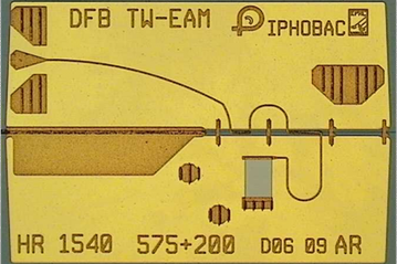
High speed integrated photonic components
Fabrication of integrated high performance compact photonics devices is a very challenge work, which needs to push semiconductor processing technology boundaries.
RISE has expertise on fabricate of monolithically integrated photonics components, for instance, analog optical transmitters /transceivers. The transmitter can be fabricated by monolithic integration of a DFB laser and a travelling wave electro-absorption modulator (DFB TW-EAM), and the transceiver can be composed by a semiconductor optical amplifier (SOA) and a reflective electro-absorption transceiver (EAT).
For more information:
RISE
Integration and packaging
The pressure to improve integration techniques has intensified during the past years: Consumer and high performance devices and systems keep becoming more compact, incorporating imaging components with increasing pixel counts and decreasing pixel pitches. Integration covers a large range of technologies and processes.
RISE has worked long time on bumping technologies and design and fabrication of various micro-lenses based on polymer, glass/quartz and semiconductor or materials.
For more information:
RISE
Light emitting components
Better and better performance light emitting devices (lasers and LEDs) are always demanded in many civil and military applications.
RISE can design and fabricate various customized 1D or 2D light emitting components working in UV, visible and infrared regimes based on III-V semiconductor quantum structures, such as quantum wells wires and dots.
For more information:
RISE

Online sensor system for resource-effective water management
Ensuring high water quality is a large and global challenge that sets high demands on sensor performance regarding sensitivity, robustness and accuracy. A broad approach is needed to enable development of a complete solution for online monitoring of water quality.
RISE with partners establish a test-bed using various sensors. The functionality of the sensor network and optimization of data handling are main focuses in this project. Additionally, services that can be linked to this system as well as models for integrating these services in existing infrastructure will be developed.
For more information:
RISE
Bio- Analysis
Miniaturisation of biomedical tools with integrated lab-on-chip solutions speed up the analysis and reduces the sample volume.
RISE has expertise in microfluidic solutions and integrated sensor technologies, and can offer
- Microfluidic solutions
- Integrated sensors
- Chip manufacturing
For more information:
RISE
Sensors embedded in machine parts
Tool manufacturing will be revolutionized by introduction of a new generation of machine parts. The functionality is enhanced by surface treatments for high wear resistance, optimized friction properties and by embeded sensors or other intelligence.
RISE develops new technologies for hybrid manufacturing, coatings and tribology control and surface embedded sensors, and also the new business and organizational models needed in next generation manufacturing industry.
For more information:
RISE
Silicon Carbide power device fabrication
Power electronics based on novel Silicon Carbide (SiC) devices are very useful for higher efficiency, smaller size and high temperature operation.
RISE has been active in SiC field since 1993, which covered all aspects technology from device design to epitaxy and device manufacturing. RISE and the spin off company Ascatron can offer power system studies, device design and manufacturing, especially SiC epitaxy service.
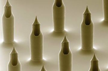
Needles for painless drug injection
It is highly desirable to intradermally inject drugs in a painless, controlled and reproducible manner. A method to achieve this is through microneedles combined with an insertion/infusion system.
KTH has developed an array of hollow microneedles , which makes it possible to inject drugs - from small molecules to large peptides. The solution is refined and commercialized by Debiotech under the name Nanoject.
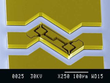
Microswitches for RF range frequencies
Modern telecommunication systems operate at high frequencies, in the RF range. The devices needed must be cheap to manufacture, which makes standard semiconductor and microsystem technology highly desirable.
KTH develops unconventional transmission-line based switch designs for a wide range of specialized applications, including interlocking mechanically multistable switches with low power consumption.
For more information:
KTH
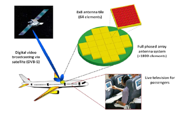
Automotive radar
Automotive radar sensors will provide means to lower the number of car accidents. The radar technology is robust and reliable in all weather conditions and over large distance and speed ranges.
KTH participates in development of automotive radar systems in the 77 GHz range, providing a possibility to steer the radar beam, a compact size and high performance at a potentially low production cost.
For more information:
KTH
Sensing secrete from single cells
Biological processes are dynamic and involve the interactions of cells with each other and their environment. To study the dynamics of cell signaling, measurements at the single cell level are necessary, since biochemical response of large cell populations are smeared out.
KTH has developed a photonic lab-on-achip sensor integrated to create a nano-photonic sensor to study the biomolecule secretion of single cells in real-time.
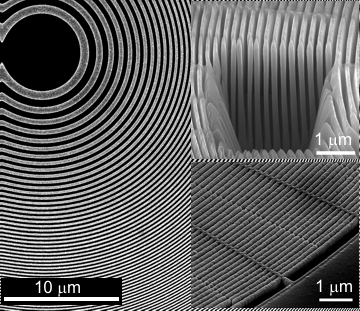
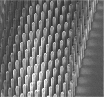
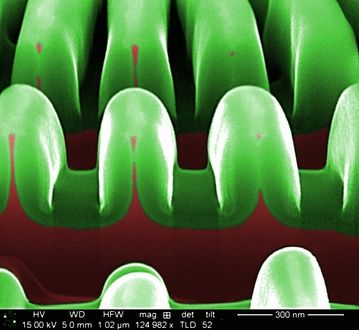
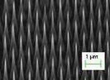
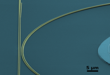
Nanofocusing X-ray zone plates
Nano beam x-ray imaging employed at synchrotron and free-electron laser facilities enables in-situ and in-operandi experiments in challenging physical environments, offering a direct correlation between material structures and physical properties.
KTH designs and manufactures x-ray zone plates with diffraction-limited resolution in the 10 - 100 nm range, for nano beam imaging for soft and hard x-rays. The fabrication is based on electron beam lithography and high aspect ratio precision etching.
For more information:
KTH
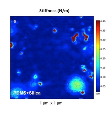
Protective nanocomposite coatings
Silica nanoparticle filled PDMS (a silicon-based organic polymer) coatings on steel have shown promise in reducing corrosion in harsh environments. Here, detailed analysis of the mechanical properties (stiffness and adhesion) of the “interphase” at the boundary between particle and polymer matrix is helping to shed light on the mechanism of protection. This study was performed using atomic force microscopy (AFM) with Intermodulation – a pioneering technique developed at KTH.
For more information:
KTH