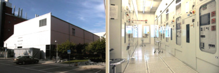
General information
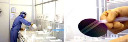
The process laboratory occupies the major part of the cleanroom area. The process laboratory is devided into 14 different lab rooms designed for different purposes, some of them are described in more detail below. The cleanroom classification ranges from class 10.000 down to class 100 areas. The class 100 areas are divided into four lab room with a total area of 105 m².
It is also possible to create local areas that are even cleaner (class 10) with different special arrangements.
Diffusion, oxidation and ion implantation
The heart in MSL's diffusion capacity is the ten vertical Koyo furnaces. The furnaces can handle 3,4 and 6 inch wafers and up to 25 wafers can be processed simultaneously in one furnace. The most common process in this area is silicon oxidation. The other available processes are boron diffusion, phosphorus diffusion, polysilicon CVD, gate oxidation, silicon nitride CVD and high temperature amd metallic annealing.
For ion implantation MSL uses an Eaton challanger 200MC ion implanter.
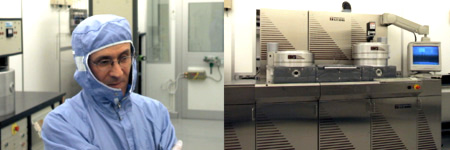
Lithography and mask making
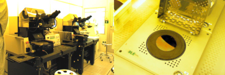
The Ångström microstructure laboratory uses a Micronic LRS-18 for mask manufacturing. The vast majority of the masks produced are 5 inch masks for research and developement. The lithography section uses a wide range of Photoresists; for example Shipley S 1813, Clariant AZ 4562, MicroChem SU8 and Shipley SPR 5740. For mask aligning and exposure MSL uses two Karl Süss MA6/BA6 mask aligners, one of them is equiped for double sided alignment.
Thin-film deposition
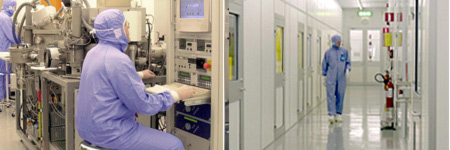
MSL offers possibility to deposit a wide range of materials with different deposition methods. Both evapouration (two Edwards Auto 306, one with electron beam evapouration) and sputtering (a VonArdenne 730S) can be used. Materials possible to deposit are for example Al, Zr, Ti, W, Ni and Mo.
Dry etching
This process field is focused around a double chambered PlasmaTherm SLR DRIE. Both silicon and metals can be etched in very high aspect-ratio structures. This is obtained by a cyclic three-step process combining passivation, sputtering and reactive ion etching. MSL also offers equipment for dry dielectrica etching (SiO2, Si3N4) and oxygene-plasma treatment; so called "ashing" or "de-scumming".
Wet chemistry
Chemical processes plays a very important role in both semiconductor research, developement and production. One of the major differenses between semiconductor processing and common manufacturing processes is that chemicals are doing the jobs instead of drills, saws, screwdrivers and other tools. For example, instead of drilling a hole in material one exposes the material to an etchant through a mask. The etchant reacts with the material and the reaction pruducts are dissolved in the etch bath. The Ångström microstructure laboratory offers for example silicon etching with KOH or KOH+IPA as standard processes.