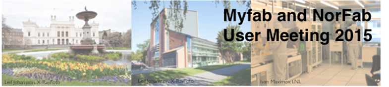
Myfab and NorFab User Meeting 2015
Lund Nano Lab, Lund, 21-22 April
Welcome to attend and contribute to the Myfab and NorFab User Meeting 2015 at Lund Nano Lab, Lund University, 21 – 22 April! This is the fourth Myfab user meeting and the second joint meeting with Norwegian NorFab. We look forward to two days of interesting presentations, visit to the Lund Nano Lab, technical workshops and presentations of your work at the poster session.
The registration is now closed.
QUESTIONS/CONTACT
Questions about the user meeting should be directed to:
· Thomas Swahn, thomas.swahn@chalmers.se,
· Cristina Andersson, cristina.andersson@chalmers.se or
· Ivan Maximov, ivan.maximov@ftf.lth.se
We look forward to meeting you!
Thomas Swahn, Director Myfab and Kay Gastinger, Director NorFab
www.myfab.se | www.norfab.no